


01 Why Puzzle
After the circuit board is designed, components need to be placed on the SMT chip assembly line. Each SMT processing factory will specify the most appropriate size of the circuit board according to the processing requirements of the assembly line. For example, the size is too small or too large, and the assembly line is fixed. The tooling of the circuit board cannot be fixed.
Then the question arises, what if the size of our circuit board itself is smaller than the size given by the factory? That is, we need to put together a circuit board and assemble multiple circuit boards into a whole piece. Imposition can significantly improve efficiency both for high-speed placement machines and for wave soldering.
02 Puzzle Description
○ Dimensions
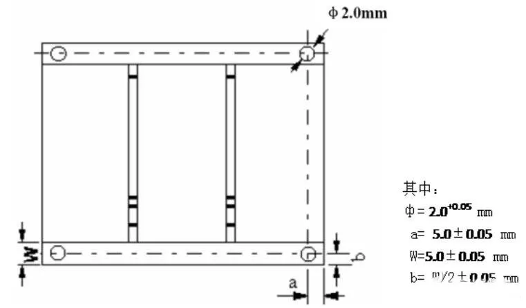
a. For the convenience of processing, the veneer board angle or craft edge should be R-type chamfer. Generally, the rounded corner diameter is Φ5.
b. When the board size is less than 100mm × 70mm, the PCB should be assembled (see Figure 3.1).
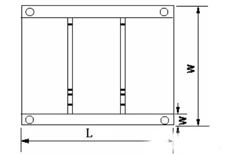
Dimension requirements of the puzzle:
Length L: 100mm ~ 400mm
Width W: 70mm ~ 400mm
○ Irregular PCB
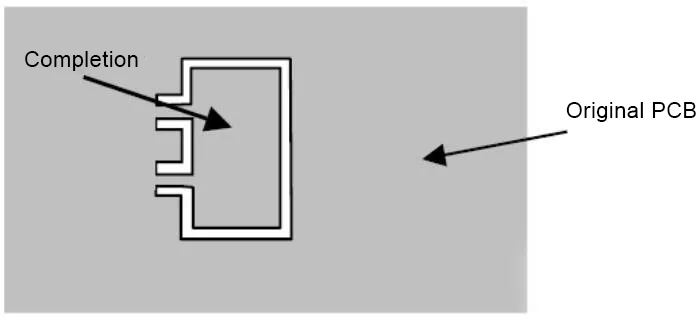
PCBs with irregular shapes and no jigs should have craft edges. If the PCB has holes with a size greater than or equal to 5mm × 5mm, the holes must be completed during the design to avoid soldering and deformation of the board during soldering. The complementary part and the original PCB part should be on one side Connect and remove it after wave soldering (see Figure 3.2)
When the connection between the process edge and the PCB is a V-shaped groove, the distance between the outer edge of the device and the V-shaped groove is ≥2mm; when the connection between the process edge and the PCB is a stamp hole, devices and lines are not allowed to be arranged within 2mm around the stamp hole.
○ Puzzle
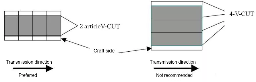
The direction of the jigsaw should be designed parallel to the direction of the conveying edge. When the size cannot meet the above requirements for the size of the imposition, the exception is. Generally requires “V-CUT” or the number of stamp hole lines ≤ 3 (except for slender veneers), see Figure 3.4
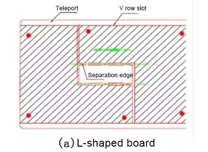
For the special-shaped board, pay attention to the connection between the daughter board and the daughter board, and try to make the connection at each step separated on a line, as shown in Figure 3.5.
03 pcb puzzle top ten matters needing attention
Under normal circumstances, PCB production will be called the so-called Panelization (Panelization) operation, the purpose is to increase the production efficiency of the SMT production line, then PCB PCB, what details should we pay attention to? Let ’s take a look together.
1. The outer frame (clamping edge) of the PCB puzzle should adopt a closed loop design to ensure that the PCB puzzle will not be deformed after it is fixed on the fixture.
2. The shape of the PCB puzzle is as close to a square as possible. It is recommended to use 2 × 2, 3 × 3,….
3. PCB panel width ≤260mm (SIEMENS line) or ≤300mm (FUJI line); if automatic dispensing is required, PCB panel width × length≤125mm × 180mm.
4. Each small board in the PCB puzzle must have at least three positioning holes, 3 ≤ aperture ≤ 6 mm, wiring or patching is not allowed within 1 mm of edge positioning holes.
5. The center distance between the small plates is controlled between 75mm ~ 145mm.
6. When setting the reference positioning point, usually leave a solderless area 1.5mm larger than the positioning point.
7. There should be no large devices or protruding devices near the connection points between the outer frame of the puzzle and the inner small board, and between the small board and the small board, and there should be more than 0.5mm of space between the edges of the components and the PCB To ensure that the cutting tool runs normally.
8. Four positioning holes are opened at the four corners of the outer frame of the panel, and the hole diameter is 4mm ± 0.01mm; the strength of the hole must be moderate to ensure that it will not break during the upper and lower plates. .
9. The reference symbols used for PCB positioning and fine-pitch device positioning. In principle, QFPs with a pitch of less than 0.65mm should be set at their diagonal positions; the positioning reference symbols used for imposition PCB daughter boards should be paired Use, place diagonally to the positioning element.
10.Large components should have positioning posts or positioning holes, focusing on I / O interface, microphone, battery interface, micro switch, headphone interface, motor, etc.