


Both the buck circuit and the boost circuit are important circuits in hardware design, especially for intelligent ONUs and OLT devices. The VOICE function in ONU design uses the boost circuit to directly boost the voltage and supply power to external phones. The best way to understand the boost circuit is to fully understand the voltage and current of each part of the circuit, Encountering some problems can clearly pinpoint the problem point. For example, what happens when the inductance increases? What happens when the capacitance increases? What is the impact of working frequency? Next, our company will explain to you.
First of all, let's talk about the most basic working principle of the BOOST circuit: In the figure below, the MOS transistor is a switch. As long as the speed is fast enough (the switching frequency is high enough), the on and off time (charging and discharging time) is well controlled, and combined with the output filter capacitor, a basically stable Vo can be obtained (the voice voltage of our intelligent ONU is generally 48V), which is the output voltage.
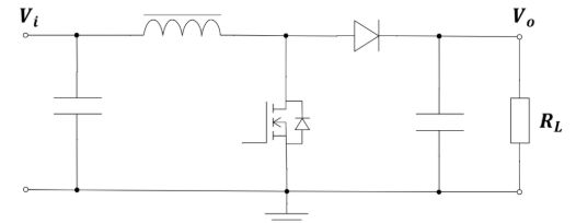
When the switch is on, the inductor L is grounded, the diode is cut off, and Vi charges the inductor L. The voltage at both ends of the inductor is Vi (usually 12V for ONU power supply). When the switch becomes non conductive, because the inductor L has already been charged and there is current flowing through it, the current at both ends of the inductor cannot suddenly change. Therefore, a voltage will be induced to make the diode on the right conduct. The output voltage Vo is constant, and the diode conduction voltage drop is Vd, so the voltage at the right end of the inductor is Vo+Vd, and the voltage at the left end of the inductor is the power input Vi. This is a boost circuit, so Vo+Vd>Vi, the inductance is discharged at this time, supplying power to the load, and charging the output filter capacitor.
When the switch becomes non conductive, because the inductor L has already been charged and there is current flowing through it, the current at both ends of the inductor cannot suddenly change. Therefore, a voltage will be induced to make the diode on the right conduct.
The output voltage Vo is constant, and the diode conduction voltage drop is Vd, so the voltage at the right end of the inductor is Vo+Vd, and the voltage at the left end of the inductor is the power input Vi. This is a boost circuit, so Vo+Vd>Vi, the inductance is discharged at this time, supplying power to the load, and charging the output filter capacitor.
The above is a brief overview of BOOST Circuit, which can serve as a reference for everyone. Our company has a strong technical team and can provide professional technical services for customers. At present, our company has diversified products: intelligent onu, communication optical module, optical fiber module, sfp optical module, olt equipment, Ethernet switch and other network equipment. If you need, you can have a deep understanding.