


Firstly, let's take a look at the general design diagram of WiFi RF circuits: (The WiFi design diagram is generally divided into these modules, with the blue area of RTL8192FR integrated in the MCU)
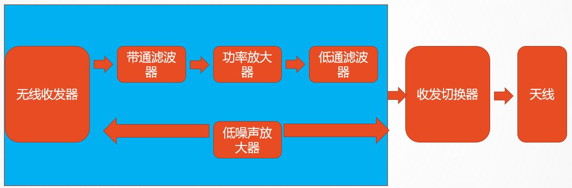
Differential signal processing: Generally, WiFi RF signals are processed using differential signal processing to increase anti-interference ability. In other words, the transceiver will send the signal in differential form, and the external circuit must also provide input for the differential RF signal to the transceiver
There are two different ways to handle it here:
1. By using a balancer, the differential signal with a phase difference of 180 ° is merged into a single ended RF signal after passing through the balancer.
2. Discrete components
What is the differential signal received by the transceiver? The signal received by the transceiver comes from the low noise amplifier in the front-end. Like the power amplifier, the low noise amplifier also processes single ended RF signals. Therefore, we must convert the signal output by the low noise amplifier. The received signal and the transmitted signal of the transceiver are almost inverse processes of each other, so the circuit structure is also similar to the opposite.
The above is a brief overview of the WIFI Design Summary - Barron, which can be used as a reference for everyone. Our company has a strong technical team and can provide professional technical services to customers. At present, our company has diversified products: intelligent onu, communication optical module, optical fiber module, sfp optical module, olt equipment, Ethernet switch and other network equipment. If you need, you can learn more about them.