


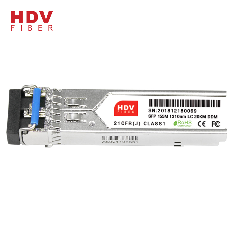

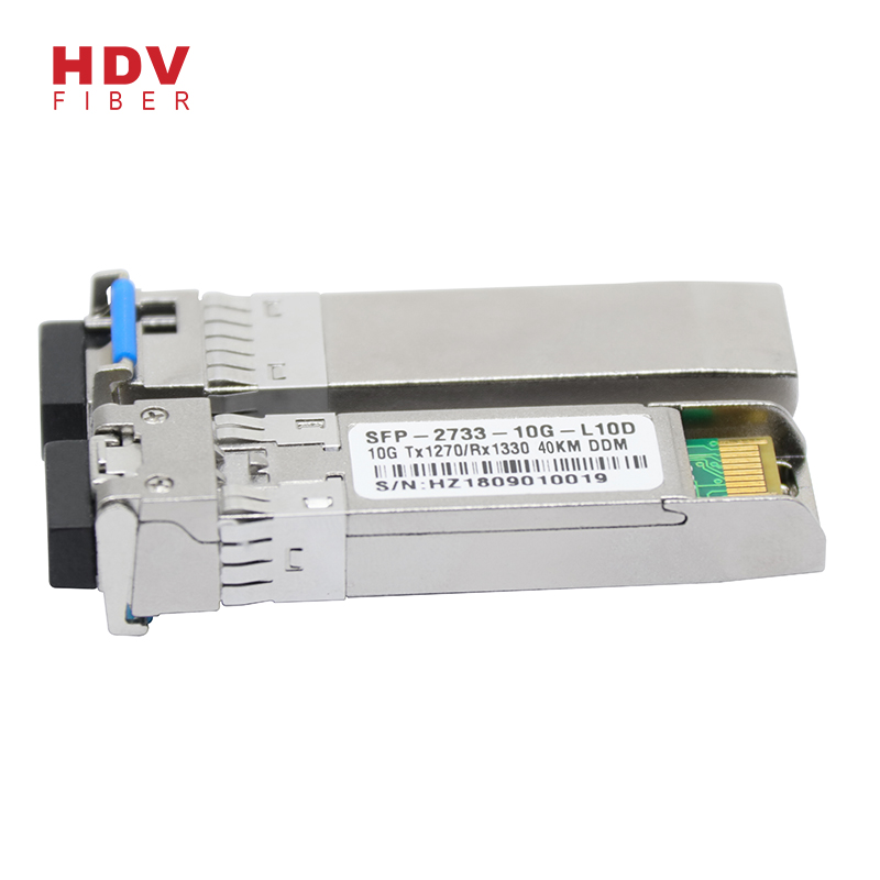
High Quality Sfp Double Fiber Transceivers - 155m Lc 1310nm Dual Fiber 20km Fiber Optic Transceiver Sfp Module – HDV Detail:
Applications
Switch
Video monitor system Telecommunication system
Absolute Maximum Ratings
| Parameter | Symbol | Min | Max | Unit | |
| Storage Temperature | TS | -40 | +85 | ℃ | |
| Operating Temperature | TOP | Commercial level | -20 | +70 | ℃ |
| industrial level | -40 | 85 | |||
| Supply Voltage | VCC | -0.5 | +4.5 | V | |
| Voltage on Any Pin | VIN | 0 | VCC | V | |
| Soldering Temperature ,Time | - | 260℃, 10 S | ℃,S | ||
Recommended Operating Conditions
| Parameter | Symbol | Min. | Typ | Max. | Unit | |
| Ambient Temperature | TAMB | Commercial level | 0 | - | 70 | ℃ |
| industrial level | -40 | 85 | ||||
| Power Supply Voltage | V CC-VEE | 3 | 3.3 | 3.6 | V | |
Operating Conditions
1 Transmitter(T=25℃, Vcc=3~3.6V (+3.3V)) 155M
| Parameter | Symbol | Min. | Typ | Max. | Unit | |||
| Center Wavelength | FP | 1280 | 1310 | 1340 | ||||
| Spectral width | △l | FP@RMS | - | 4 | 6 | nm | ||
| Side Mode Suppression Ratio | SMSR (DFB only) | 30 | dB | |||||
| Output Power | 0~30km | 1310 FP | Po | -12 | - | -0 | dBm | |
| Extinction Ratio | ER | 155M | 10 | - | dB | |||
| Supply Current | ICCT | - | 150 | mA | ||||
| Input Differential Impedance | Rin | 100 | Ω | |||||
| Data Input Swing Differential | Vin | 300 | 1200 | mV | ||||
| Optical Modulation Amplitude | OMA | 174 | μW | |||||
| Transmit Disable Voltage | VD | 2.0 |
Vcc |
V | |
| Transmit Enable Voltage | VEN | 0 |
0.8 |
V | |
| Transmit Disable Assert Time |
10 |
us | |||
| Optical Rise/Fall Time | Tr/ Tf (20-80%) | 400 |
8000 |
ps | |
| Output Optical Eye | IUT-T G.957 Compliant | ||||
2 Receiver (T=25℃, Vcc=3~3.6V (+3.3V) 155M
| Parameter | Symbol | Min. | Typ | Max. | Unit | |||
| Wavelength Range | lc | 1100 | 1610 | nm | ||||
| Sensitivity | 0~30km | 155M | Pin | PMIN | - | -35 | -34 | dBm |
| MAX. Input Power (Saturation) | PMAX | -0 | - | - | ||||
| Signal Detect Assert | PA | - | - | -34 | ||||
| Signal Detect De-assert | PD | -44 | - | - | ||||
| Signal Detect Hysteresis | PHYS | 1 | - | 4 | ||||
| Supply Current | ICCR | - | - | 150 | mA | |||
| Data Output Swing Differential | Vout | 400 | - | 1000 | mV | |||
| Signal Detect Voltage – High | VSDHC | 2.0 | - | VCC | V | |||
| Signal Detect Voltage – Low | VSDL | 0 | - | 0.8 | ||||
Notes:
switch from a high state to a low state.
1)Value of output power and sensitivity can be customized according to the demand
Ordering Information
Example
DSFP 3X 03-F 1 1 LC - 20
| Sign | Mean | Description | |||||
| DSFP | Module type | DSFP= Dual fibers SFP | SFP=Single fiber SFP | ||||
| 3X | Center wave | 3X=1310tx/1100~1610 rx | 5X=1550tx/1100~1610 rx | CWDM Like 49=1490 CWDM TX 1100~1610 RX | |||
| 03 | date Rate | 03=155M | 12=622M | 24=1.25G |
48=2.5G |
60=3.125G | |
| F | Laser type | F=FP | D=DFB |
C=CWDM |
V=VCSEL | ||
| 1 | Operating T | 1=-20~+70℃ | 2=-40~+85℃ | ||||
| 1 | DDMI | 1=NO DDM | 2=DDMI | ||||
| LC | Connector | SC=SC | LC=LC | ||||
| 20 | Distance | 022=220M | 055=550M |
5=5KM |
10=10KM | ||
| 20=20KM | 40=40KM |
80=80KM |
100=100KM | ||||
Typical products
| Part No. | Wavelength | Con- nector | Temp. | TXPower (dBm) | RX Sens(Max.) (dBm) | DD MI | Distance |
| DSFP3X03-F11LC-20 | T 1310FP/rx 1100~1610 | LC | -20 to 70 | -12 to-0 | -34 | F | 20km |
Designing notice
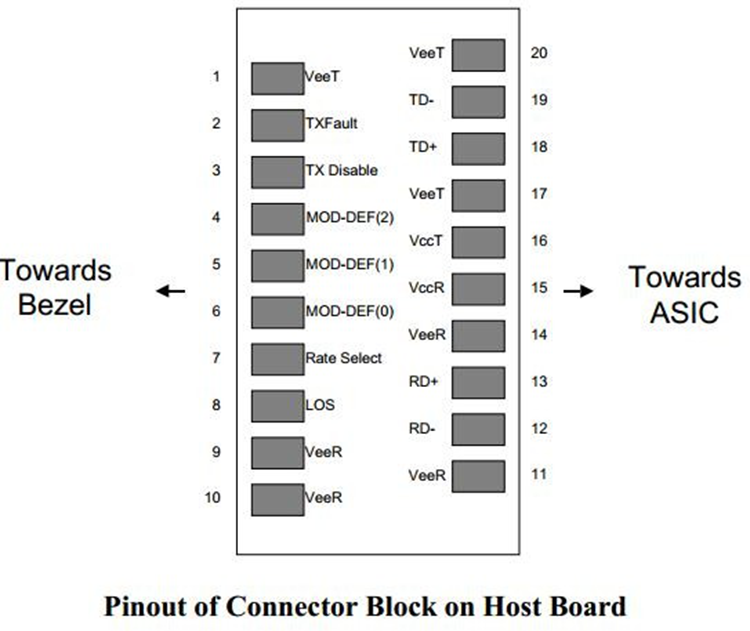
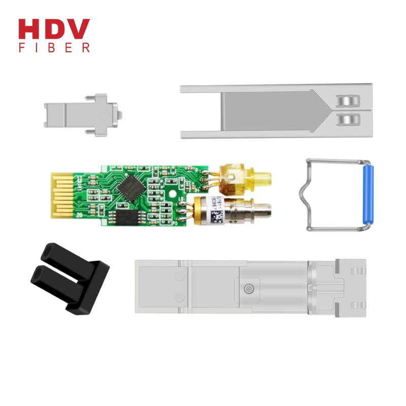
DSFP Pin description
|
Pin |
Descriptions |
Pin |
Descriptions |
|
1 |
VEET |
Transmitter Ground (Common with Receiver Ground) |
1 |
|
2 |
TFAULT |
Transmitter Fault. |
2 |
|
3 |
TDIS |
Transmitter Disable. Laser output disabled on high or open. |
3 |
|
4 |
MOD_DEF(2) |
Module Definition 2. Data line for Serial ID. |
4 |
|
5 |
MOD_DEF(1) |
Module Definition 1. Clock line for Serial ID. |
4 |
|
6 |
MOD_DEF(0) |
Module Definition 0. Grounded within the module. |
4 |
|
7 |
Rate Select |
No connection required |
|
|
8 |
LOS |
Loss of Signal indication. Logic 0 indicates normal operation. |
5 |
|
9 |
VEER |
Receiver Ground (Common with Transmitter Ground) |
1 |
|
10 |
VEER |
Receiver Ground (Common with Transmitter Ground) |
1 |
|
11 |
VEER |
Receiver Ground (Common with Transmitter Ground) |
1 |
|
12 |
RD- |
Receiver Inverted DATA out. AC Coupled |
|
|
13 |
RD+ |
Receiver Non-inverted DATA out. AC Coupled |
|
|
14 |
VEER |
Receiver Ground (Common with Transmitter Ground) |
1 |
|
15 |
VCCR |
Receiver Power Supply |
|
|
16 |
VCCT |
Transmitter Power Supply |
|
|
17 |
VEET |
Transmitter Ground (Common with Receiver Ground) |
1 |
|
18 |
TD+ |
Transmitter Non-Inverted DATA in. AC Coupled. |
|
|
19 |
TD- |
Transmitter Inverted DATA in. AC Coupled. |
|
|
20 |
VEET |
Transmitter Ground (Common with Receiver Ground) |
1 |
Small Form-factor Pluggable (SFP) Transceiver MultiSource Agreement (MSA)
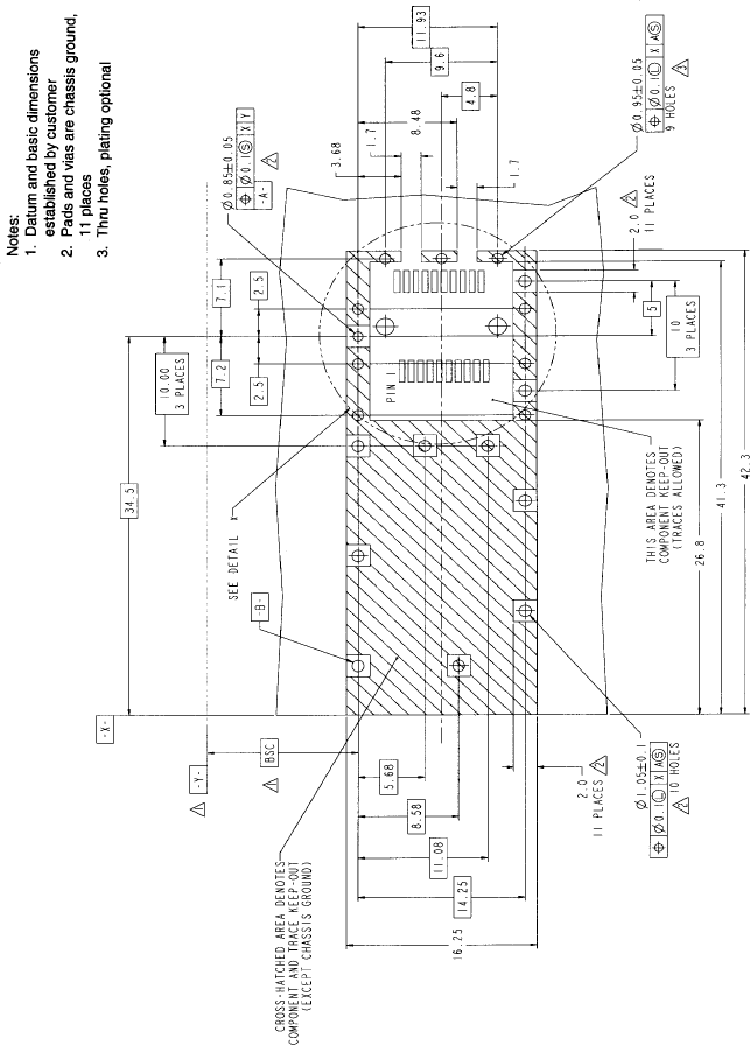
SFP Host Board Mechanical Layout
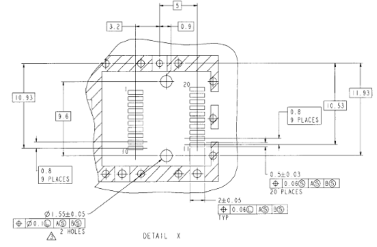
Figure 6 SFP Host Board Mechanical Layout (Cont.)
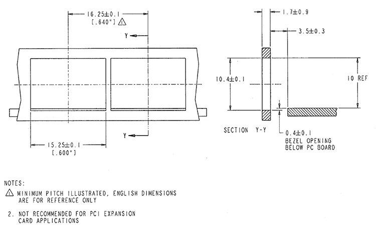
Recommended Bezel Design
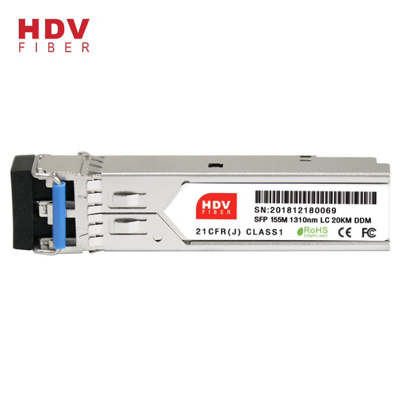
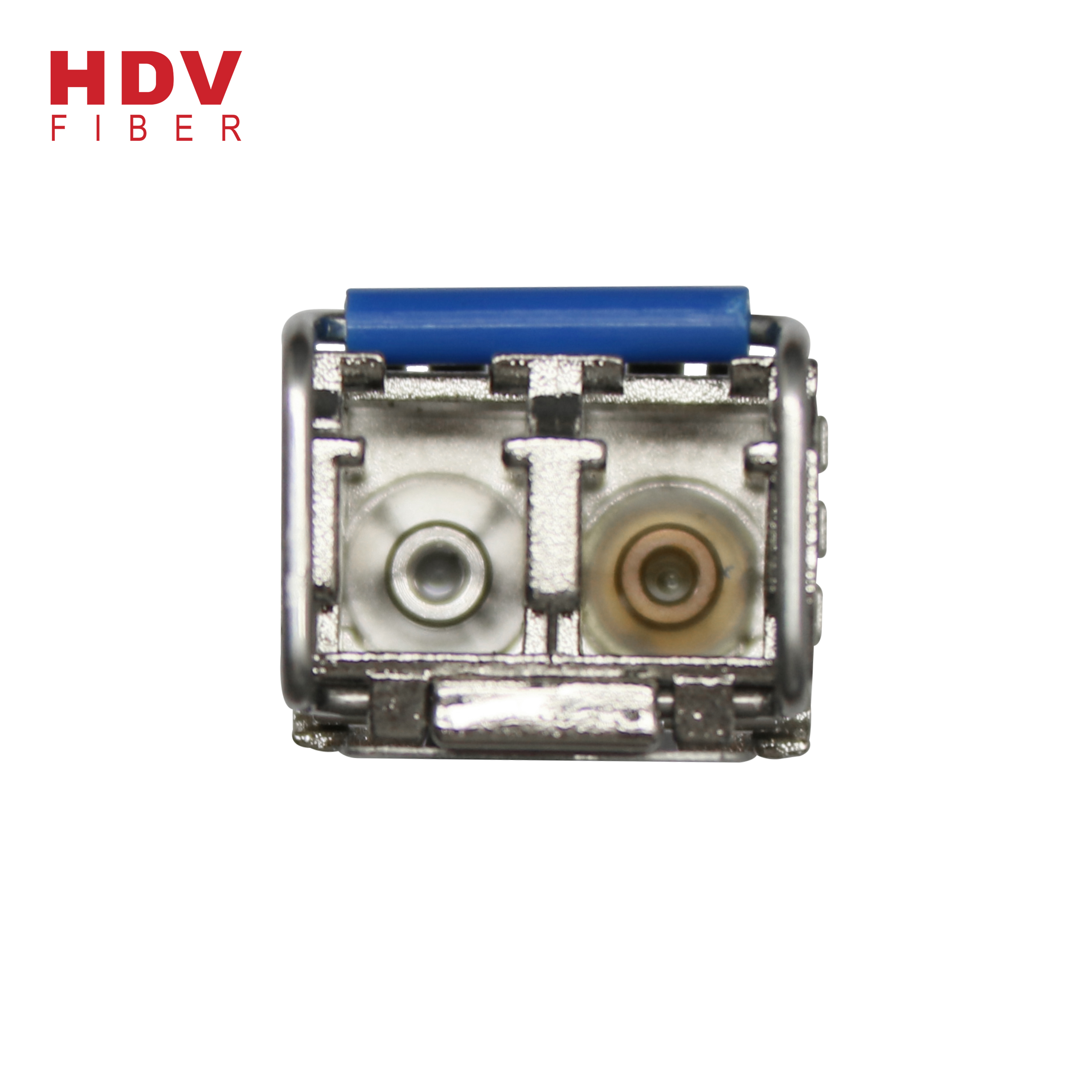
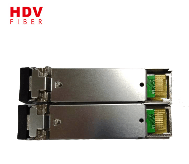
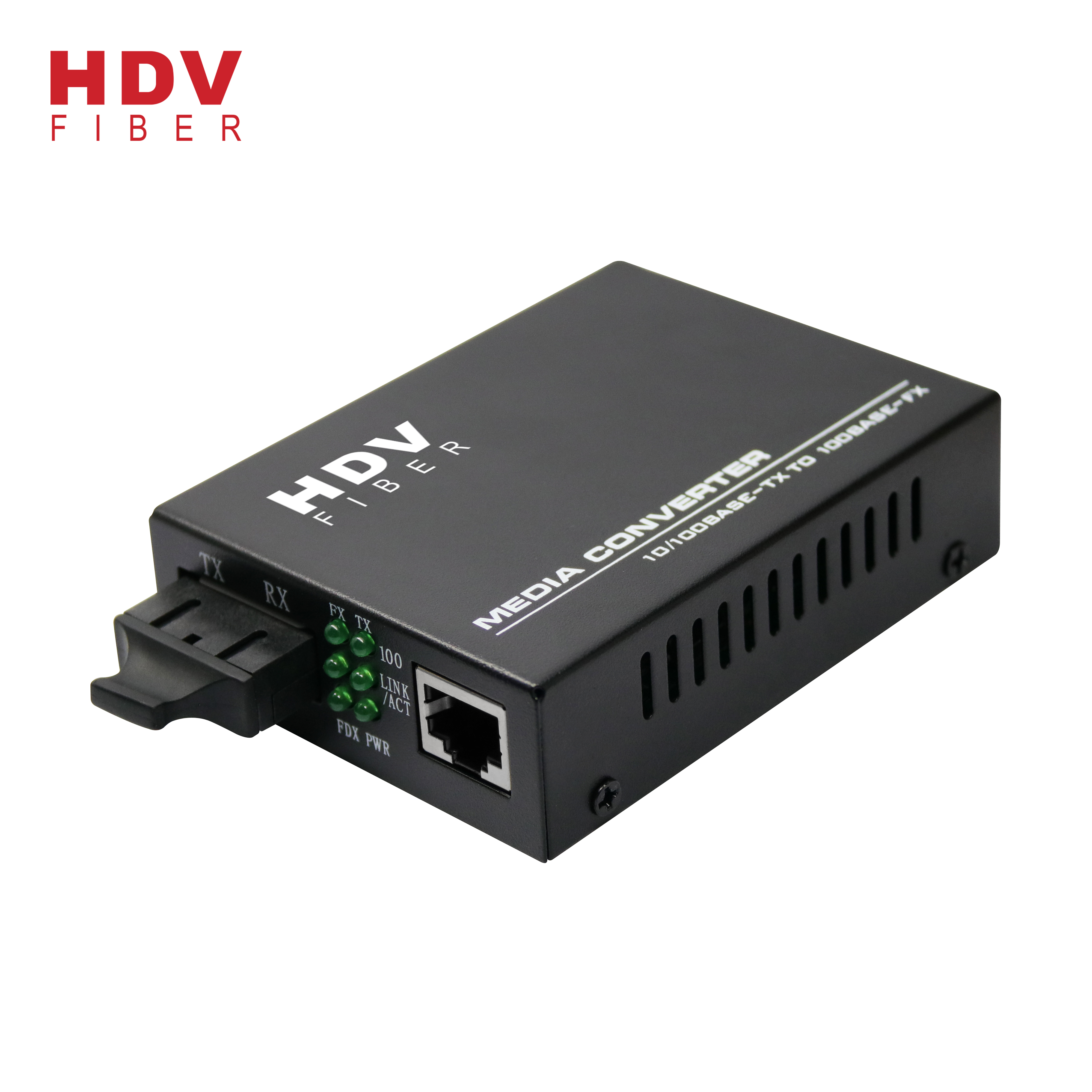
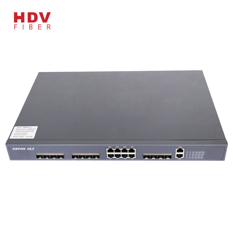
Product detail pictures:
Related Product Guide:
Menara Networks announces availability of new OTN tunable SFP+ for commercial and industrial temperature applications | Second Hand Onu
嵌入式PON光链路层监测 确保FTTH网络高效运维 | Second Hand Onu
During the past few years, our business absorbed and digested state-of-the-art technologies the two at home and abroad. Meanwhile, our firm staffs a group of experts devoted to your development of High Quality Sfp Double Fiber Transceivers - 155m Lc 1310nm Dual Fiber 20km Fiber Optic Transceiver Sfp Module – HDV , The product will supply to all over the world, such as: Czech republic, Florence, Venezuela, Our production have been exported to more than 30 countries and regions as first hand source with lowest price. We sincerely welcome customers from both at home and abroad to come to negotiate business with us.
It is not easy to find such a professional and responsible provider in today's time. Hope that we can maintain long-term cooperation.
Products categories
-1.jpg)

Write your message here and send it to us