


Notes:
switch from a high state to a low state.
1)Value of output power and sensitivity can be customized according to the demand
1)Value of output power and sensitivity can be customized according to the demand
Ordering Information:
- Example
- DSFP 8X 24-C 1 2 LC - 055
|
Sign |
Mean |
Description |
||||||
|
DSFP |
Module type |
DSFP= Dual fibers SFP |
SFP=Single fiber SFP |
|||||
|
8x |
Center wave |
30=1310tx/NO rx |
50=1550tx/NO RX |
8X=850TX any RX |
||||
|
24 |
date Rate |
03=155M |
12=622M |
24=1.25G |
48=2.5G |
60=3.125G |
||
|
V |
Laser type |
F=FP |
D=DFB |
C=CWDM |
V=VCSEL |
|||
|
1 |
Operating T |
1=-20~+70℃ |
2=-40~+85℃ |
|||||
|
1 |
DDMI |
1=NO DDM |
2=DDMI |
|||||
|
LC |
Connector |
SC=SC |
LC=LC |
|||||
|
055 |
Distance |
022=220M |
055=550M |
5=5KM |
10=10KM |
|||
|
20=20KM |
40=40KM |
80=80KM |
100=100KM |
|||||
Designing notice:
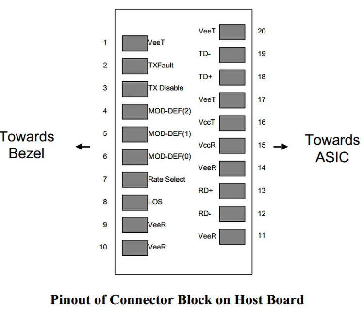
DSFP Pin description
|
Pin |
Descriptions |
Pin |
Descriptions |
|
1 |
VEET |
Transmitter Ground (Common with Receiver Ground) |
1 |
|
2 |
TFAULT |
Transmitter Fault. |
2 |
|
3 |
TDIS |
Transmitter Disable. Laser output disabled on high or open. |
3 |
|
4 |
MOD_DEF(2) |
Module Definition 2. Data line for Serial ID. |
4 |
|
5 |
MOD_DEF(1) |
Module Definition 1. Clock line for Serial ID. |
4 |
|
6 |
MOD_DEF(0) |
Module Definition 0. Grounded within the module. |
4 |
|
7 |
Rate Select |
No connection required |
|
|
8 |
LOS |
Loss of Signal indication. Logic 0 indicates normal operation. |
5 |
|
9 |
VEER |
Receiver Ground (Common with Transmitter Ground) |
1 |
|
10 |
VEER |
Receiver Ground (Common with Transmitter Ground) |
1 |
|
11 |
VEER |
Receiver Ground (Common with Transmitter Ground) |
1 |
|
12 |
RD- |
Receiver Inverted DATA out. AC Coupled |
|
|
13 |
RD+ |
Receiver Non-inverted DATA out. AC Coupled |
|
|
14 |
VEER |
Receiver Ground (Common with Transmitter Ground) |
1 |
|
15 |
VCCR |
Receiver Power Supply |
|
|
16 |
VCCT |
Transmitter Power Supply |
|
|
17 |
VEET |
Transmitter Ground (Common with Receiver Ground) |
1 |
|
18 |
TD+ |
Transmitter Non-Inverted DATA in. AC Coupled. |
|
|
19 |
TD- |
Transmitter Inverted DATA in. AC Coupled. |
|
|
20 |
VEET |
Transmitter Ground (Common with Receiver Ground) |
1 |
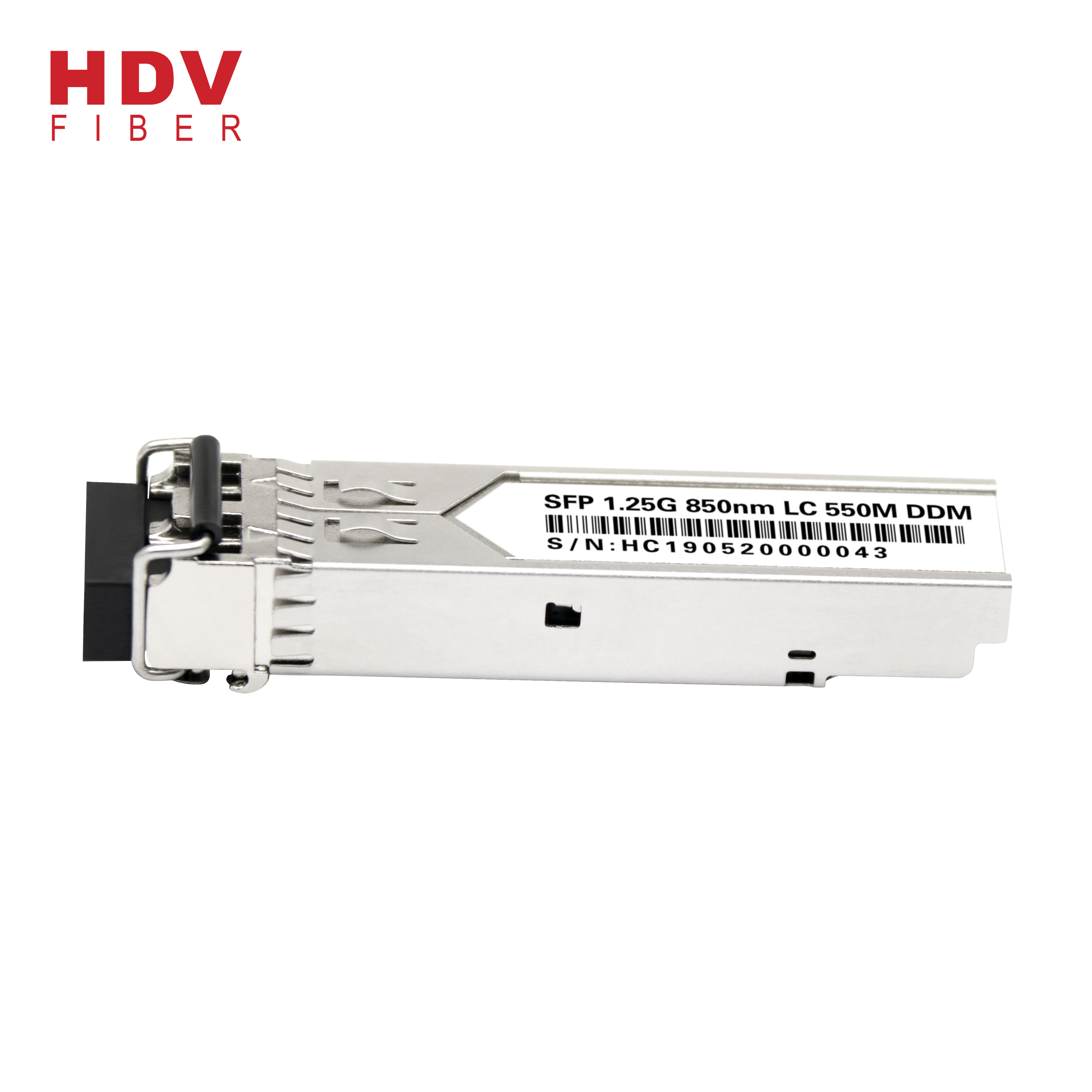
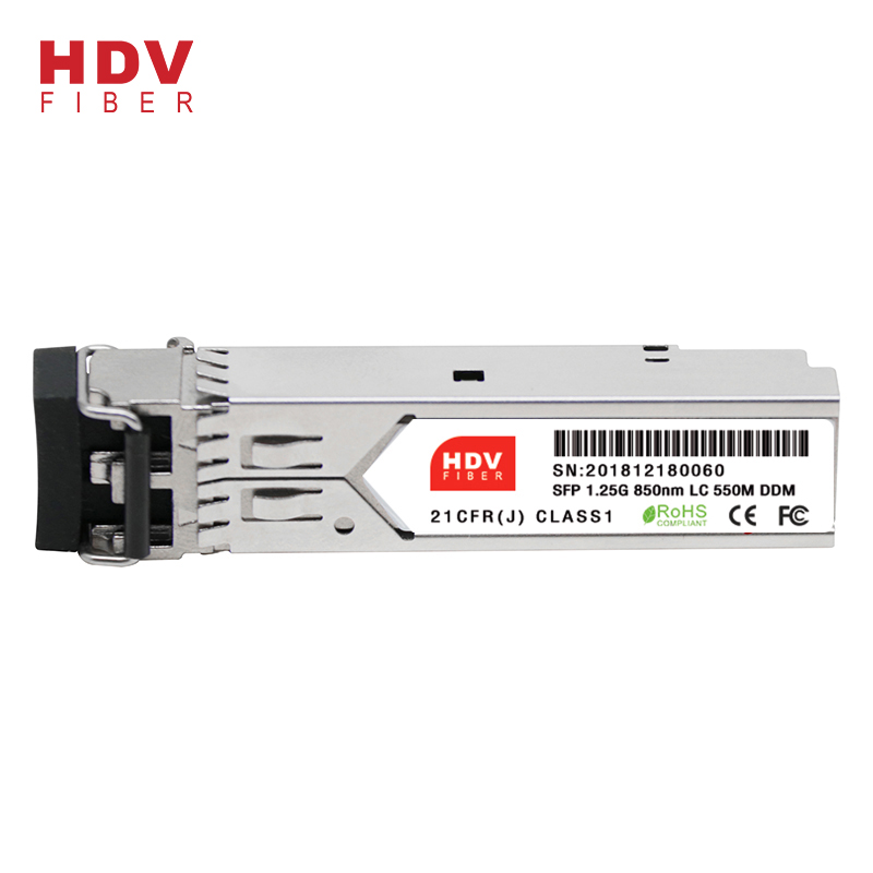
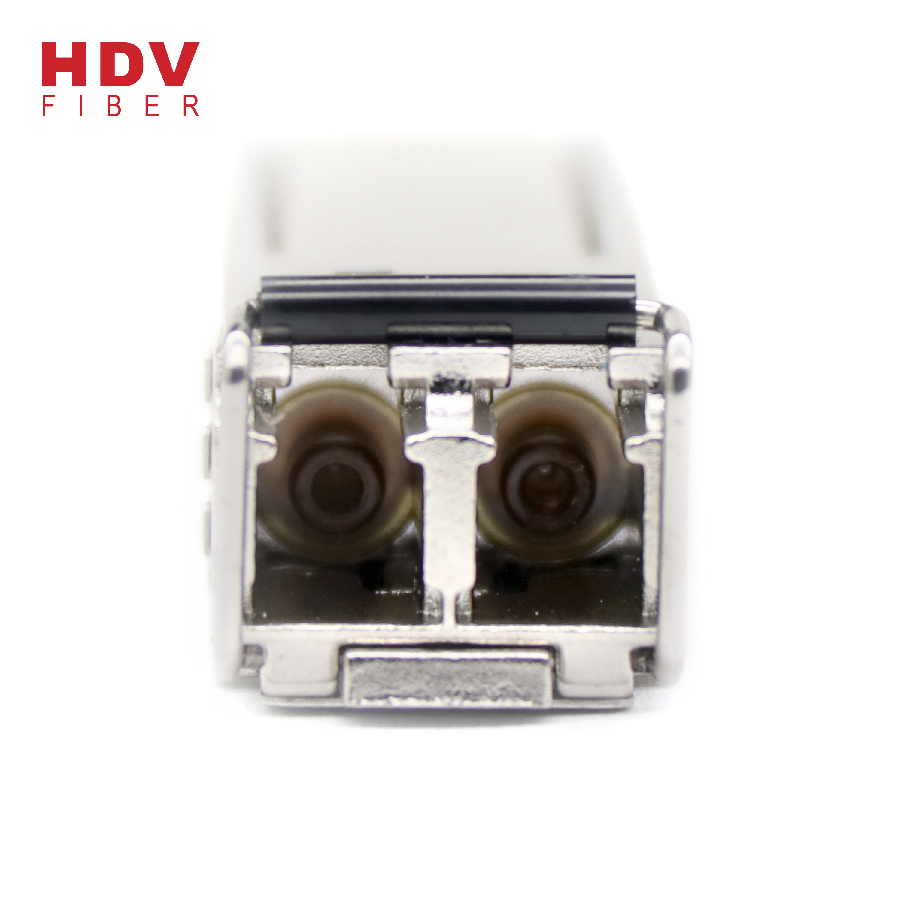
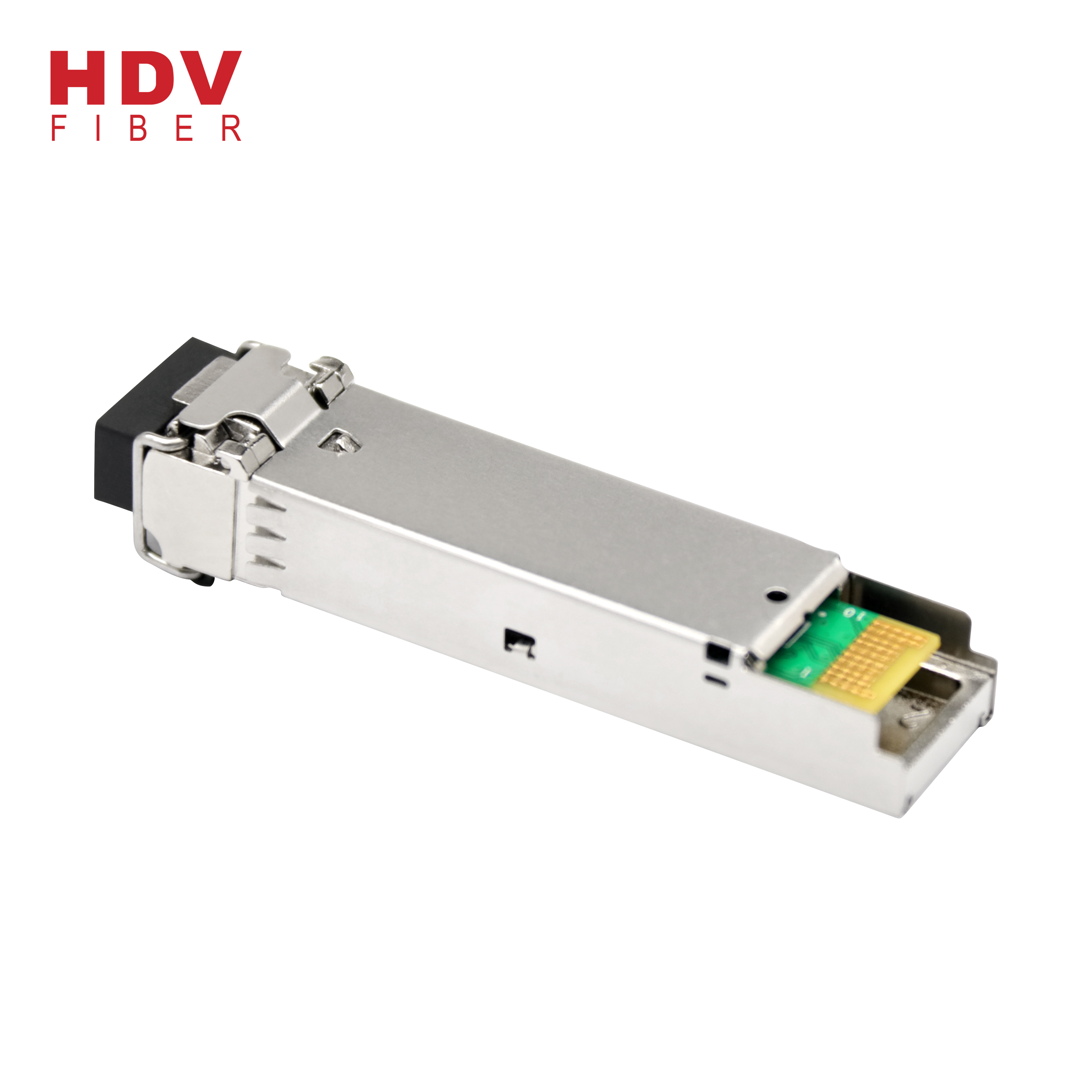
Small Form-factor Pluggable (SFP) Transceiver MultiSource Agreement (MSA)
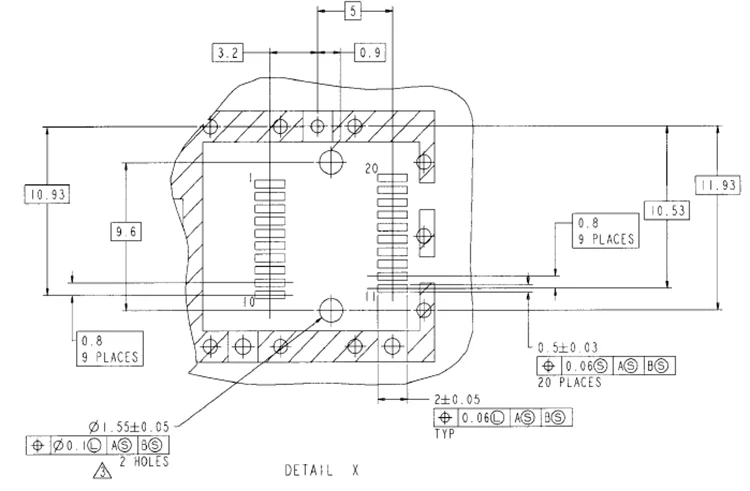
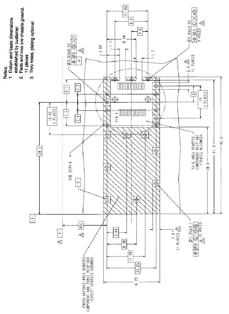
SFP Host Board Mechanical Layout
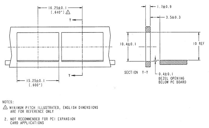
Recommended Bezel Design
Absolute Maximum Ratings:
|
Parameter |
Symbol |
Min |
Max |
Unit |
|
|
Storage Temperature |
TS |
-40 |
+85 |
℃ |
|
|
Operating Temperature |
TOP |
Commercial level |
-20 |
+70 |
℃ |
|
industrial level |
-40 |
85 |
|||
|
Supply Voltage |
VCC |
-0.5 |
+4.5 |
V |
|
|
Voltage on Any Pin |
VIN |
0 |
VCC |
V |
|
|
Soldering Temperature ,Time |
- |
260℃, 10 S |
℃,S |
||
Recommended Operating Conditions:
|
Parameter |
Symbol |
Min. |
Typ |
Max. |
Unit |
|
|
Ambient Temperature |
TAMB |
Commercial level |
0 |
- |
70 |
℃ |
|
industrial level |
-40 |
85 |
||||
|
Power Supply Voltage |
V CC-VEE |
3 |
3.3 |
3.6 |
V |
|
Operating Conditions:
1.Transmitter(T=25℃, Vcc=3~3.6V (+3.3V)) 1.25G
|
Parameter |
Symbol |
Min. |
Typ |
Max. |
Unit |
|||
|
Center Wavelength |
lc |
840 |
850 |
860 |
nm |
|||
|
Spectral width |
△l |
VICSEL@RMS |
- |
0.85 |
nm |
|||
|
Output Power |
0~550m |
850 |
Po |
-9 |
- |
-3 |
dBm |
|
|
Extinction Ratio |
ER |
1.25G |
9 |
- |
dB |
|||
|
Supply Current |
ICCT |
- |
150 |
mA |
||||
|
Input Differential Impedance |
Rin |
100 |
Ω |
|||||
|
Data Input Swing Differential |
Vin |
300 |
1200 |
mV |
||||
|
Optical Modulation Amplitude |
OMA |
174 |
μW |
|||||
|
Transmit Disable Voltage |
VD |
2.0 |
Vcc |
V |
||||
|
Transmit Enable Voltage |
VEN |
0 |
0.8 |
V |
||||
|
Transmit Disable Assert Time |
10 |
us |
||||||
|
Optical Rise/Fall Time |
Tr/ Tf (20-80%) |
150 |
260 |
ps |
||||
|
Deterministic Jitter Contribution |
TX ΔDJ |
51.7 |
ps |
|||||
|
Total Jitter Contribution |
TX ΔTJ |
90 |
ps |
|||||
|
Output Optical Eye |
IUT-T G.957 Compliant |
|||||||
2.Receiver (T=25℃, Vcc=3~3.6V (+3.3V) 1.25G
|
Parameter |
Symbol |
Min. |
Typ |
Max. |
Unit |
|||
|
Wavelength Range |
lc |
760 |
860 |
nm |
||||
|
Sensitivity |
0~550m |
1.25G |
Pin |
PMIN |
- |
-18 |
-17 |
dBm |
|
MAX. Input Power (Saturation) |
PMAX |
-3 |
- |
- |
||||
|
Signal Detect Assert |
PA |
- |
- |
-20 |
||||
|
Signal Detect De-assert |
PD |
-24 |
- |
- |
||||
|
Signal Detect Hysteresis |
PHYS |
1 |
- |
4 |
||||
|
Supply Current |
ICCR |
- |
- |
150 |
mA |
|||
|
Data Output Swing Differential |
Vout |
400 |
- |
1000 |
mV |
|||
|
Signal Detect Voltage – High |
VSDHC |
2.0 |
- |
VCC |
V |
|||
|
Signal Detect Voltage – Low |
VSDL |
0 |
- |
0.8
|
||||
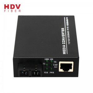
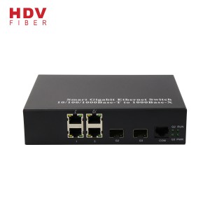
- Switch
- Video monitor system
- Telecommunication system
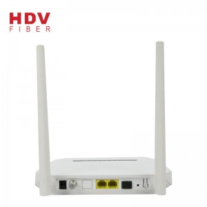
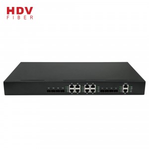
Products categories

Write your message here and send it to us