The through-hole itself has parasitic capacitance to the ground. If the diameter of the isolation hole on the floor layer of the through-hole is known to be D2, the diameter of the through-hole pad is D1, the thickness of the PCB board is T, and the dielectric constant of the board substrate is ε, The parasitic capacitance of the via is approximately C=1.41 ε TD1/(D2-D1)
The main impact of parasitic capacitance on the circuit caused by vias is that it prolongs the signal time and reduces the speed of the circuit. For example, for a PCB board with a thickness of 50 Mil, if a vias with an inner diameter of 10 Mil and a pad diameter of 20 Mil are used, and the distance between the pad and the copper area on the ground is 32 Mil, we can approximately calculate the parasitic capacitance of the vias using the above formula as follows: C=1.41 x 4.4x 0.050 x 0.020/(0.032-0.020)=0.517pF, The rise time variation caused by this capacitance is: T10-90=2.2C (Z0/2)=2.2x0.517x (55/2)=31.28ps. From these values, it can be seen that although the parasitic capacitance of a single via may not have a significant effect on slowing down the rise, caution should be exercised if vias are used multiple times in the wiring for interlayer switching.
Along with the parasitic capacitance in the via, there is also a parasitic inductance. The parasitic series inductance weakens the contribution of the bypass capacitance and weakens the filtering effectiveness of the entire power system. The following formula can be used to simply calculate an approximate parasitic inductance in the via:
L=5.08h [ln (4h/d)+1], where L refers to the inductance of the through hole, h is the length of the through hole, and d is the diameter of the central drilling hole. From the equation, it can be seen that the diameter of the via has a small impact on the inductance, while the length of the via has the greatest impact on the inductance. Using the above example, the inductance of the via can be calculated as L=5.08x0.050 [ln (4x0.050/0.010)+1]=1.015nH. If the rise time of the signal is 1ns, then its equivalent impedance size is: XL=π L/T10-90=3.19 Ω.
In summary:
Choosing a thinner PCB is beneficial for reducing parasitic parameters
Try not to change layers or use unnecessary vias for signal routing
Drill holes near the power supply and ground, and the shorter and thicker the wiring of the holes and pins, the better
Place more ground holes near the signal switching layer to provide the closest circuit for the signal
When making a series of optical fiber products, such as optical module, ONU, optical fiber module, OLT module, etc., you must consider the impact of vias on bosa, transmitting eye diagram, extinction ratio, etc., or the impact on receiving sensitivity
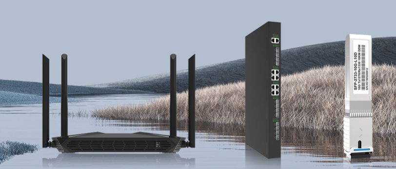
The above is a brief overview of "Introduction to Key Parameters of BOSA - via size (II)", which can be used as a reference. Our company has a quite strong technical team and can provide professional technical services to customers. At present, our company has diversified products: intelligent onu, communication optical module, optical fiber module, sfp optical module, olt equipment, Ethernet switch and other network equipment. If you need, you can learn more about them.