


Notes:
1. TX Fault is an open collector output, which should be pulled up with a 4.7k~10kΩ resistor on the host board to a voltage
between2.0V and Vcc+0.3V. Logic 0 indicates normal operation; logic 1 indicates a laser fault of some kind. In the low state,
the output will be pulled to less than 0.8V.
2. TX Disable is an input that is used to shut down the transmitter optical output. It is pulled up within themodule
witha 4.7k~10kΩ resistor. Its states are:
Low (0~0.8V): Transmitter on
(>0.8V, <2.0V): Undefined
High (2.0~3.465V): Transmitter Disabled
Open: Transmitter Disabled
3. MOD-DEF 0,1,2 are the module definition pins. They should be pulled up with a 4.7k~10kΩ resistor on
the host board. The pull-up voltage shall be VccT or VccR.
MOD-DEF 0 is grounded by the module to indicate that the module is present
MOD-DEF 1 is the clock line of two wire serial interface for serial ID
MOD-DEF 2 is the data line of two wire serial interface for serial ID
4. LOS is an open collector output, which should be pulled up with a 4.7k~10kΩ resistor on the host board to a voltage
between2.0Vand Vcc+0.3V. Logic 0 indicates normal operation; logic 1 indicates loss of signal. In the low state, the
output will be pulled to less than 0.8V.
5. These are the differential receiver output. They are internally AC-coupled 100Ω differential lines which should be terminated
with 100Ω (differential) at the user SERDES.
6. These are the differential transmitter inputs. They are AC-coupled, differential lines with 100Ω differential termination inside the module.
6. These are the differential transmitter inputs. They are AC-coupled, differential lines with 100Ω differential termination inside the module.
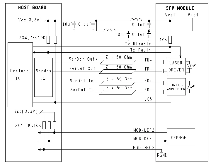
Recommended Application Circuit:
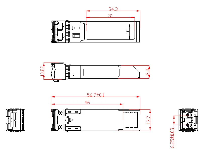
Outline drawing (mm):
Ordering information :
|
Part No. |
Wavelength |
Connector |
Temp. |
TX Power (dBm) |
RX Sens (Max.) (dBm) |
Distance |
|
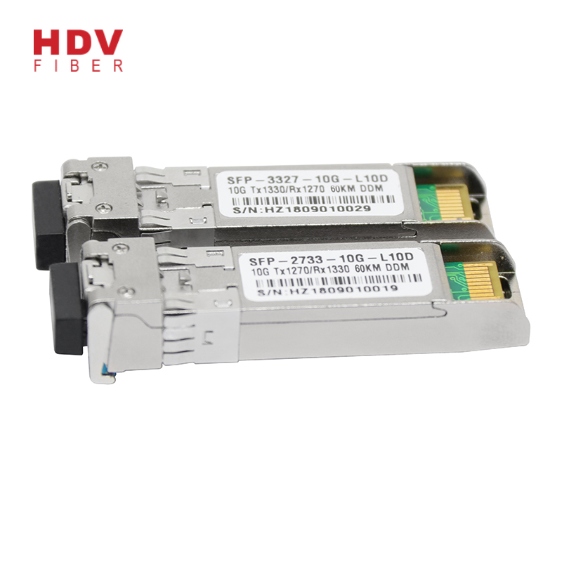
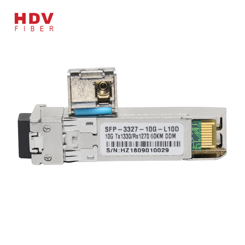
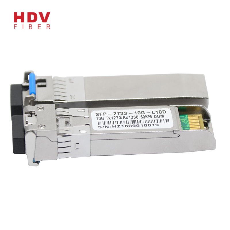
BSFP+-10G-L10A |
1270TX/1330RX |
LC |
0~70°C |
-5 to 0 |
-14 |
10km |
|
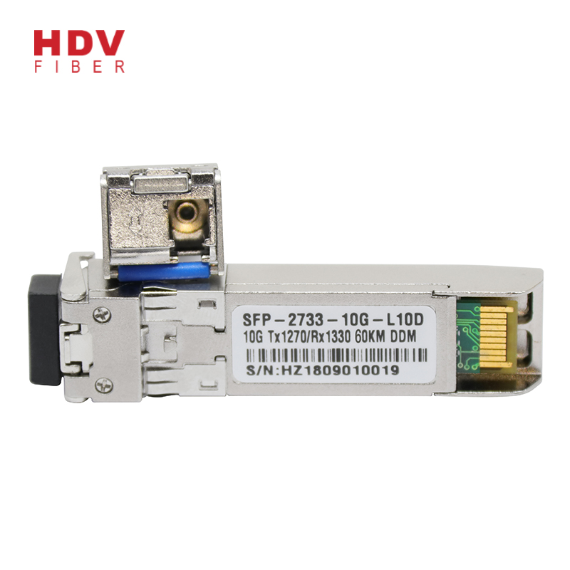
BSFP+-10G-L10B |
1330TX/1270RX |
LC |
0~70°C |
-5 to 0 |
-14 |
10km |
|
BSFP+-10G-L20A |
1270TX/1330RX |
LC |
0~70°C |
-2to 3 |
-14 |
20km |
|
BSFP+-10G-L20B |
1330TX/1270RX |
LC |
0~70°C |
-2to 3 |
-14 |
20km |
|
BSFP+-10G-L40A |
1270TX/1330RX |
LC |
0~70°C |
+1 to +5 |
-17 |
40km |
|
BSFP+-10G-L40B |
1330TX/1270RX |
LC |
0~70°C |
+1 to +5 |
-17 |
40km |
|
BSFP+-10G-L60A |
1270TX/1330RX |
LC |
0~70°C |
+1 to +6 |
-20 |
60km |
|
BSFP+-10G-L60B |
1330TX/1270RX |
LC |
0~70°C |
+1 to +6 |
-20 |
60km |
Absolute Maximum Ratings:
|
Parameter |
Symbol |
Min |
Max |
Unit |
|
|
Storage Temperature |
TS |
-40 |
+85 |
℃ |
|
|
Operating Temperature |
TOP |
Commercial level |
-20 |
+70 |
℃ |
|
industrial level |
-40 |
85 |
|||
|
Supply Voltage |
VCC |
-0.5 |
+3.6 |
V |
|
|
Voltage on Any Pin |
VIN |
0 |
VCC |
V |
|
|
Soldering Temperature ,Time |
- |
260℃, 10 S |
℃,S |
||
Operation Environment:
|
Parameter |
Symbol |
Min. |
Typ |
Max. |
Unit |
|
|
Ambient Temperature |
TAMB |
Commercial level |
0 |
- |
70 |
℃ |
|
industrial level |
-40 |
85 |
||||
|
Power Supply Voltage |
V CC-VEE |
3.15 |
3.3 |
3.45 |
V |
|
|
Power Dissipation |
1 |
W |
||||
|
Data Rate |
10GBASE-LR |
10.3125 |
Gbps |
|||
Optical Characteristics:
(Ambient Operating Temperature 0C to +70C, Vcc =3.3 V)
|
Parameter |
Symbol |
Min. |
Typ. |
Max. |
Units |
||||
|
Transmitter Section |
|||||||||
| Center Wavelength |
lo |
1260 |
1270 |
1280 |
nm |
||||
|
1320 |
1330 |
1340 |
|||||||
| RMS Spectral Width |
Dl |
- |
- |
1 |
nm |
||||
| Side Mode Suppression Ratio |
SMSR |
30 |
dB |
||||||
| Average Output Power | 10km |
Po |
-5 |
- |
0 |
dBm |
|||
| 20km |
-2 |
+3 |
|||||||
| 40km |
+1 |
+5 |
|||||||
| 60km |
+1 |
+6 |
|||||||
| Extinction Ratio |
Er |
3.5 |
- |
- |
dB |
||||
| Dispersion Penalty |
2 |
dB |
|||||||
| Input Differential Impedance |
Zin |
90 |
100 |
110 |
Ω |
||||
| Relative Intensity Noise |
RIN12OMA |
-128 |
dB/Hz |
||||||
| Total jitter |
Tj |
0.28 |
UI(p-p) |
||||||
|
Receiver Section |
|||||||||
| Center Wavelength |
lo |
1320 |
1330 |
1340 |
nm |
||||
|
1260 |
1270 |
1280 |
|||||||
|
Receiver Sensitivity |
10km |
Rsen |
-14 |
dBm |
|||||
| 20km |
-14 |
||||||||
| 40km |
-17 |
||||||||
| 60km APD |
-23 |
||||||||
|
Receiver Overload |
0~40km |
Rov |
0.5 |
dBm |
|||||
| 60KM |
-6 |
||||||||
| Return Loss |
12 |
dB |
|||||||
| LOS Assert |
LOSA |
-25 |
dBm |
||||||
| LOS Dessert |
LOSD |
-15 |
dBm |
||||||
| LOS Hysteresis |
0.5 |
4 |
dB |
||||||
| LOS | High |
2.0 |
VCC+0.3 |
V |
|||||
| Low |
0 |
0.8 |
|||||||
Electrical Characteristics:
(Ambient Operating Temperature 0C to +70C, Vcc =3.3 V)
|
Parameter |
Symbol |
Min. |
Typ. |
Max. |
unit |
|
|
Transmitter Section |
||||||
| Input Differential Impendence |
Zin |
90 |
100 |
110 |
Ohm |
|
| Data Input Swing Differential |
Vin |
180 |
700 |
mV |
||
| TX Disable | Disable |
2.0 |
Vcc |
V |
||
| Enable |
0 |
0.8 |
V |
|||
| TX Fault | Assert |
2.0 |
Vcc |
V |
||
| Deassert |
0 |
0.8 |
V |
|||
|
Receiver Section |
||||||
| Output differential impendence |
Zout |
100 |
Ohm |
|||
| Data output Swing Differential |
Vout |
300 |
800 |
mV |
||
| Rx_LOS | Assert |
2.0 |
Vcc |
V |
||
| Deassert |
0 |
0.8 |
V |
|||
Diagnostics:
|
Parameter |
Range |
Accuracy |
Unit |
Calibration |
| Temperature |
-5 ~ 75 |
±3 |
ºC |
Internal |
| Voltage |
0 ~ VCC |
0.1 |
V |
Internal |
| Bias Current |
0 ~ 12 |
0.3 |
mA |
Internal |
| Tx Power |
-8 ~ 1 |
±1 |
dBm |
Internal |
| Rx Power |
-18 ~ 0 |
±1 |
dBm |
Internal |
EEPROM INFORMATION(A0):
|
Addr |
Field Size (Bytes) |
Name of Field |
HEX |
Description |
| 0 |
1 |
Identifier |
03 |
SFP |
| 1 |
1 |
Ext. Identifier |
04 |
MOD4 |
| 2 |
1 |
Connector |
07 |
LC |
| 3-10 |
8 |
Transceiver |
10 00 00 00 00 00 00 00 |
Transmitter Code |
| 11 |
1 |
Encoding |
06 |
64B66B |
| 12 |
1 |
BR, nominal |
67 |
10000M bps |
| 13 |
1 |
Reserved |
00 |
|
| 14 |
1 |
Length (9um)-km |
00 |
|
| 15 |
1 |
Length (9um) |
00 |
|
| 16 |
1 |
Length (50um) |
08 |
|
| 17 |
1 |
Length (62.5um) |
02 |
|
| 18 |
1 |
Length (copper) |
00 |
|
| 19 |
1 |
Reserved |
00 |
|
| 20-35 |
16 |
Vendor name |
48 44 56 20 20 20 20 20 20 20 20 20 20 20 20 20 |
HDV |
| 36 |
1 |
Reserved |
00 |
|
| 37-39 |
3 |
Vendor OUI |
00 00 00 |
|
| 40-55 |
16 |
Vendor PN |
xx xx xx xx xx xx xx xx xx xx xx xx xx xx xx xx |
ASC II |
| 56-59 |
4 |
Vendor rev |
31 2E 30 20 |
V1.0 |
| 60-61 |
2 |
Wavelength |
05 1E |
1310nm |
| 62 |
1 |
Reserved |
00 |
|
| 63 |
1 |
CC BASE |
XX |
Check sum of byte 0~62 |
| 64-65 |
2 |
Options |
00 1A |
LOS, TX_DISABLE, TX_FAULT |
| 66 |
1 |
BR, max |
00 |
|
| 67 |
1 |
BR, min |
00 |
|
| 68-83 |
16 |
Vendor SN |
00 00 00 00 00 00 00 00 00 00 00 00 00 00 00 00 |
Unspecified |
| 84-91 |
8 |
Vendor date code |
XX XX XX 20 |
Year, Month, Day |
| 92-94 |
3 |
Reserved |
00 |
|
| 95 |
1 |
CC_EXT |
XX |
Check sum of byte 64~94 |
| 96-255 |
160 |
Vendor specific |
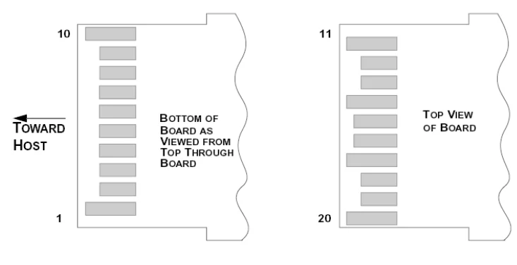
| Pins | Name |
Discription |
NOTE |
|
1 |
VeeT |
Transmitter Ground |
|
|
2 |
Tx Fault |
Transmitter Fault Indication |
1 |
|
3 |
Tx Disable |
Transmitter Disable |
2 |
|
4 |
MOD DEF2 |
Module Definition 2 |
3 |
|
5 |
MOD DEF1 |
Module Definition 1 |
3 |
|
6 |
MOD DEF0 |
Module Definition 0 |
3 |
|
7 |
RS0 |
Not Connected |
|
|
8 |
LOS |
Loss of Signal |
4 |
|
9 |
RS1 |
Not Connected |
|
|
10 |
VeeR |
Receiver Ground |
|
|
11 |
VeeR |
Receiver Ground |
|
|
12 |
RD- |
Inv. Received Data Output |
5 |
|
13 |
RD+ |
IReceived Data Output |
5 |
|
14 |
VeeR |
Receiver Ground |
|
|
15 |
VccR |
Receiver Power |
|
|
16 |
VccT |
Transmitter Power |
|
|
17 |
VeeT |
Transmitter Ground |
|
|
18 |
TD+ |
Transmit Data Input |
6 |
|
19 |
TD- |
Inv. Transmit Data Input |
6 |
|
20 |
VeeT |
Transmitter Ground |
10GBASE-LR at 10.31Gbps
10GBASE-LW at 9.95Gbps
0.6~10Gb/s CPRI/OBSAI
Other Optical Link
Products categories
-
SFP 10G bidi 1270nm/1330nm optical fiber transc...
-
10G 1550nm 40KM LC connector dual fiber optic S...
-
Huawei/cisco Compatible 10g Sfp+ lr 10km 10g Sf...
-
SFP-10G-SR SFP+ 10g 850nm 300m ddm SFP module
-
10g Spf+ 850nm Mode Dual Fiber 300m Optical Mod...
-
10G 1310nm 20KM LC connector dual fiber optic S...
Write your message here and send it to us