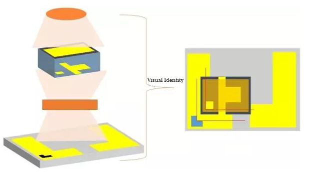
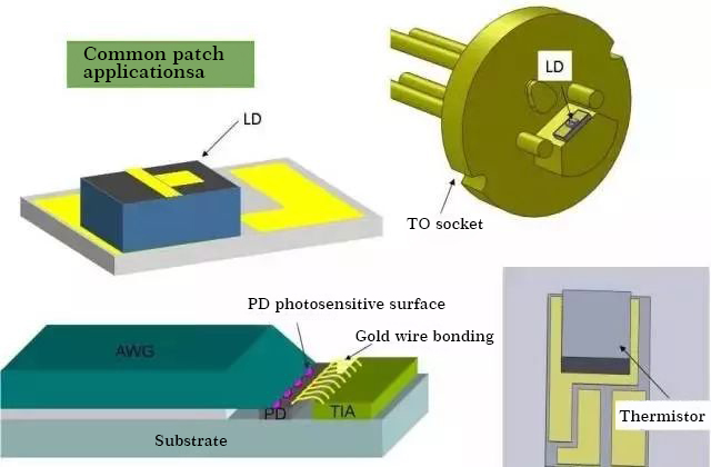
The first step in the process of receiving a chip may be the patch; a TO includes a patch that heat sinks to the TO socket, a chip that LDs to the heat sink, and a backlight PD;
The specific mounting process may be very different: the object to be attached is usually an LD / PD chip, or TIA, resistor / capacitor; the placement can be performed on an aluminum nitride heat sink or directly on the PCB; the placement Eutectic welding or conductive adhesive can be used; the patch can only require tens or even hundreds of microns of accuracy, such as TIA, resistors, and sub-micron accuracy, such as passive flip-chip welding.
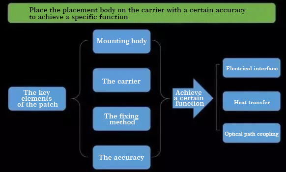
Having said all this, what exactly is a patch? There never seems to be a standardized definition. However, it can be seen from the above examples that they have one thing in common: the device is used to place and fix the placement body on the carrier with a certain accuracy to achieve a specific function. (Why use equipment? I think the placement process that can be automated is called a patch, otherwise it can only be called manual bonding.) Based on this common point, I have summarized four key elements of a patch: the placement body, the carrier , Fixed method, accuracy. And what carrier is used, what solder is selected, and what the accuracy requirements are, it depends entirely on the function that the object to be mounted needs to achieve.
Here is a look at the various possibilities contained in the four elements of the patch:
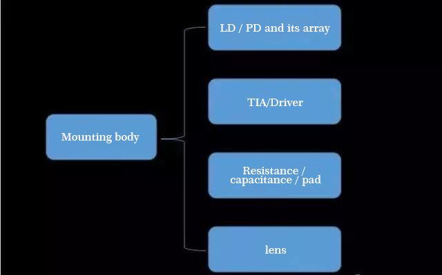
Most of the mounts are LD and PD chips.
TIA / Driver / Resistor / Capacitors, such as placement bodies that do not require high accuracy, can be manually replaced instead of large volumes.
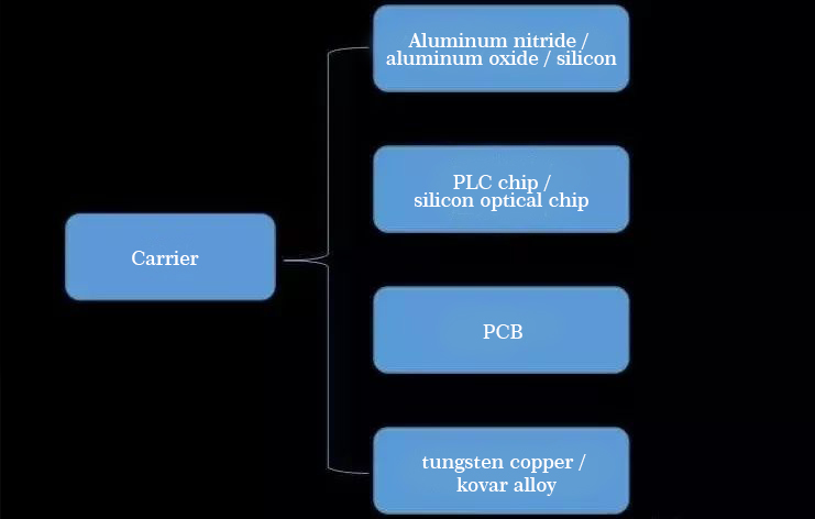
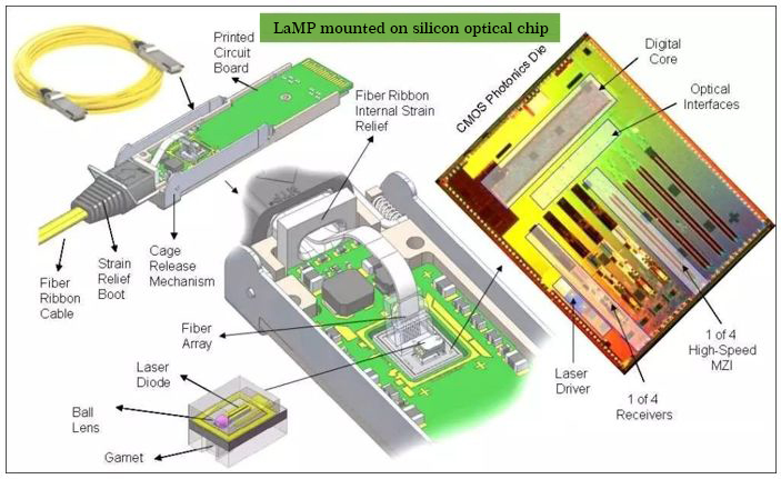
The most traditional carrier is AIN heat sink; with the development of integrated chips, PLC chips and silicon optical chips have also become common mounting bodies, such as silicon light grating coupling chips, which require LaMP to be mounted on silicon optical chips; PCB is Common carriers in COB packages, such as data communication 100G-SR4 modules, PD / VSCEL are directly mounted on the PCB.
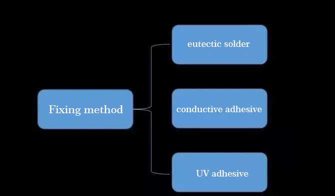
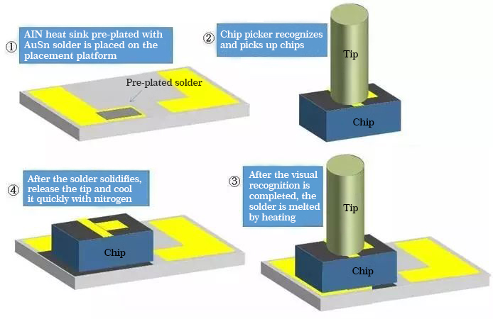
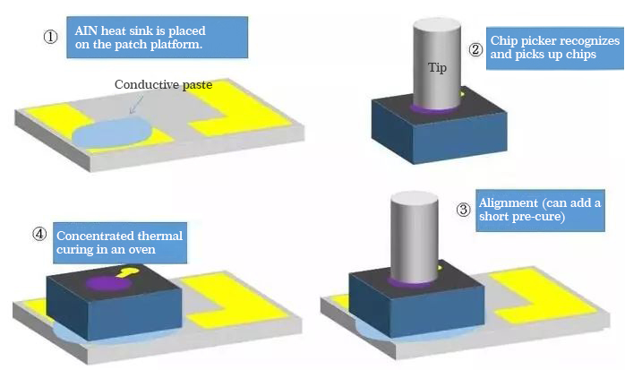
Au80Sn20 alloy is a common LD-mount eutectic solder. Conductive adhesive is often used to mount PD. UV glue fixed lens is more suitable.
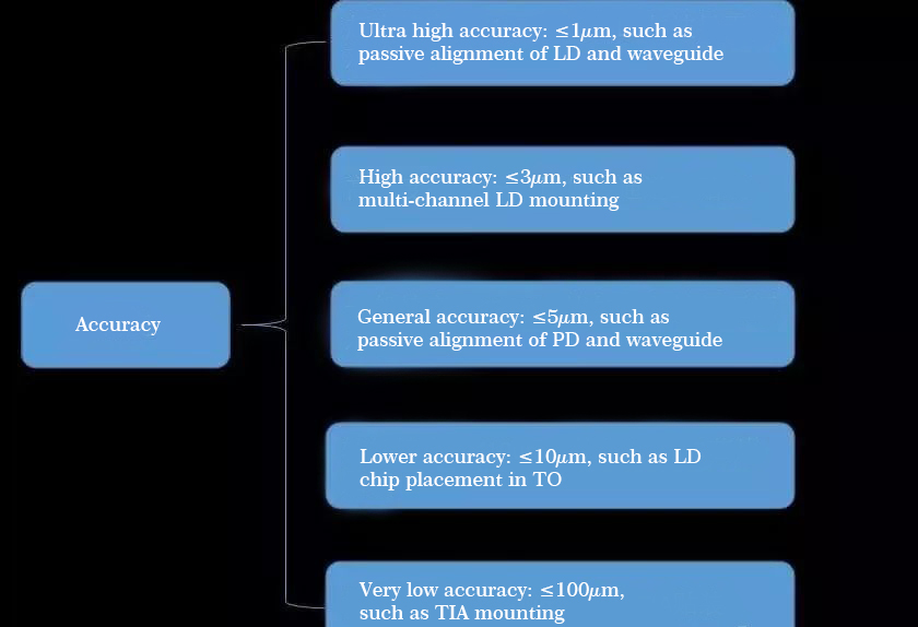
Accuracy depends on specific application;
Where optical path coupling is required, the accuracy requirement is relatively high.
Passive alignment requires higher accuracy than active coupling.
LD placement requires higher accuracy than PD placement,
TIA / resistor / capacitor don’t need any precision, just stick it.
General placement process
Gold-tin eutectic solder patch
Conductive paste patch
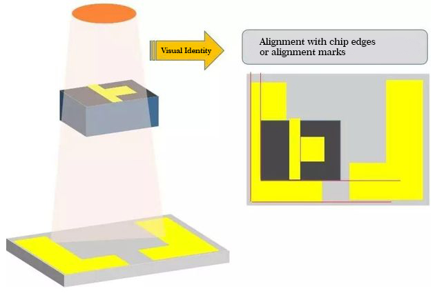
Where accuracy is not high, you only need to look down at the CCD to capture images of the chip and the substrate at the same time, and use alignment marks or chip edges to align
For flip-chip applications, multiple CCDs are also required, looking at both the bottom of the chip and the surface of the substrate. High-precision applications also require special alignment marks.